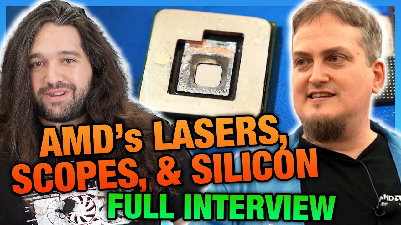
AMD's CPU Analysis Lab Full Interview Lasers, Scopes, & Silicon
video description
Date: 2023-08-28
Related videos


Comments and reviews: 20
wol
Topics Covered
- Saw Usage : The lab uses a saw to cut parts that might still be attached to boards for quick access.
- Lab Focus : The Austin lab focuses half on diagnosing issues and half on helping the design team. Another lab in Singapore focuses more on reliability.
- Oven Usage : An oven is used for a phenomenon called BTI (Bias Temperature Inversion) to redistribute trapped charges and recover parts that aren't real fails.
- Laser Profiler : Measures the bowing of the die when attached to the substrate. Useful for diagnosing issues like cracking during testing.
- Time Domain Reflectance (TDR) : Used to debug assembly issues by comparing the reflected signal from a known good unit to the unit under test. Helps in isolating problems in the substrate, die, or the interface between them.
- Package Analysis : The lab has three main functions package analysis, fault isolation, and physical failure analysis. Package analysis focuses on assembly-related issues.
- Fault Isolation : The primary focus in Austin, it involves keeping the devices electrically viable for tests while looking through the silicon. This is a non-destructive process.
- Physical Failure Analysis (PFA) : Takes over after fault isolation to do cross-sections and identify the actual defects in the silicon.
- Polishing Tools : Various tools are used for thinning the silicon to a certain thickness for high-magnification analysis. These range from hand polishers to more automated polishing wheels.
- Silicon Thinning : The lab thins the silicon from around 700 microns to as low as 50 microns for high-magnification imaging. The process is challenging due to the bowing of the die.
- CNC Milling Tools : These are used to follow the contour of the die for more precise thinning, especially when package capacitors and stiffeners cannot be removed.
- Measurement Tools : Various tools are used to measure the thickness of the silicon, both manually and automatically.
- Bulk Silicon : The material removed during the thinning process is bulk silicon. The chips are designed with the bulk silicon at the bottom and the layers of metal and transistors at the top.
- Functional Parts : Despite the thinning, the parts can remain functional, although it becomes challenging to run tests on such thin silicon without heat sinks.
- Thermal Considerations : Thinning the silicon can lead to distinct heat spots, which can cause damage. The bulk material provides thermal support.
- Polishing Requirements : Depending on the magnification needed, different polishing methods are used. For desktop and server parts, usually only the indium and backside metalization need to be polished off.
- Drilling Through the Lid : Demonstrated the capability to drill through the lid of the package for certain experiments.
- Scanning Acoustic Microscope (SAM) : Uses sonar to produce an image of the chip. It can focus on different depths within the chip and is good for finding delamination or problems with the Indium.
- Non-Destructive Analysis : The choice of machine or tool depends on the job's priority and requirements. For high-priority jobs, fewer steps might be taken to expedite the process.
- Indium Scan : Used to check for voids in the indium layer, especially for returned or failed parts, before disassembling them.
- Utility Lines : The lab has a raised floor with utility lines running underneath for power, water, and gas.
- 3D X-Ray : A future addition to the lab that will offer new possibilities for analysis.
- Breakout Boards : Custom boards with sockets that make it easier to connect to specific pins on the chip for testing.
- Thermal Mapping : Design teams often request thermal data to identify hot spots on the chip, especially for stacked die configurations.
- Laser Voltage Probing (LVP) : A laser-based technique that allows for functional testing of transistors. It doesn't measure voltage but can show data toggling through the transistor.
- High Magnification Technique : Laser Voltage Probing (LVP) requires high magnification and a thinned die to accurately aim the laser at individual transistors. Note: They are not allowed to show the microscopes that can image into the silicon with solid immersion lenses.
- Signal Detection : The technique looks at the reflected laser power and detects changes in amplitude or phase to determine if a transistor has turned on.
- Closing Remarks : The video concludes with a thank you to Jason for the walkthrough of AMD's secret lab and a note that more videos will be available showing other parts of the facilities.
reply
Topics Covered
- Saw Usage : The lab uses a saw to cut parts that might still be attached to boards for quick access.
- Lab Focus : The Austin lab focuses half on diagnosing issues and half on helping the design team. Another lab in Singapore focuses more on reliability.
- Oven Usage : An oven is used for a phenomenon called BTI (Bias Temperature Inversion) to redistribute trapped charges and recover parts that aren't real fails.
- Laser Profiler : Measures the bowing of the die when attached to the substrate. Useful for diagnosing issues like cracking during testing.
- Time Domain Reflectance (TDR) : Used to debug assembly issues by comparing the reflected signal from a known good unit to the unit under test. Helps in isolating problems in the substrate, die, or the interface between them.
- Package Analysis : The lab has three main functions package analysis, fault isolation, and physical failure analysis. Package analysis focuses on assembly-related issues.
- Fault Isolation : The primary focus in Austin, it involves keeping the devices electrically viable for tests while looking through the silicon. This is a non-destructive process.
- Physical Failure Analysis (PFA) : Takes over after fault isolation to do cross-sections and identify the actual defects in the silicon.
- Polishing Tools : Various tools are used for thinning the silicon to a certain thickness for high-magnification analysis. These range from hand polishers to more automated polishing wheels.
- Silicon Thinning : The lab thins the silicon from around 700 microns to as low as 50 microns for high-magnification imaging. The process is challenging due to the bowing of the die.
- CNC Milling Tools : These are used to follow the contour of the die for more precise thinning, especially when package capacitors and stiffeners cannot be removed.
- Measurement Tools : Various tools are used to measure the thickness of the silicon, both manually and automatically.
- Bulk Silicon : The material removed during the thinning process is bulk silicon. The chips are designed with the bulk silicon at the bottom and the layers of metal and transistors at the top.
- Functional Parts : Despite the thinning, the parts can remain functional, although it becomes challenging to run tests on such thin silicon without heat sinks.
- Thermal Considerations : Thinning the silicon can lead to distinct heat spots, which can cause damage. The bulk material provides thermal support.
- Polishing Requirements : Depending on the magnification needed, different polishing methods are used. For desktop and server parts, usually only the indium and backside metalization need to be polished off.
- Drilling Through the Lid : Demonstrated the capability to drill through the lid of the package for certain experiments.
- Scanning Acoustic Microscope (SAM) : Uses sonar to produce an image of the chip. It can focus on different depths within the chip and is good for finding delamination or problems with the Indium.
- Non-Destructive Analysis : The choice of machine or tool depends on the job's priority and requirements. For high-priority jobs, fewer steps might be taken to expedite the process.
- Indium Scan : Used to check for voids in the indium layer, especially for returned or failed parts, before disassembling them.
- Utility Lines : The lab has a raised floor with utility lines running underneath for power, water, and gas.
- 3D X-Ray : A future addition to the lab that will offer new possibilities for analysis.
- Breakout Boards : Custom boards with sockets that make it easier to connect to specific pins on the chip for testing.
- Thermal Mapping : Design teams often request thermal data to identify hot spots on the chip, especially for stacked die configurations.
- Laser Voltage Probing (LVP) : A laser-based technique that allows for functional testing of transistors. It doesn't measure voltage but can show data toggling through the transistor.
- High Magnification Technique : Laser Voltage Probing (LVP) requires high magnification and a thinned die to accurately aim the laser at individual transistors. Note: They are not allowed to show the microscopes that can image into the silicon with solid immersion lenses.
- Signal Detection : The technique looks at the reflected laser power and detects changes in amplitude or phase to determine if a transistor has turned on.
- Closing Remarks : The video concludes with a thank you to Jason for the walkthrough of AMD's secret lab and a note that more videos will be available showing other parts of the facilities.
reply
ClassicRoc
Steve while I appreciate you bringing LTT inconsistencies to light you definitely made the situation more gaslighty than you needed to. You COULD have reached out to get a comment from Linus. Of course you didn't need to but it came off as an intentional attempt to keep things hyped and THAT wasn't appreciated. You also could do better. Just don't forget no one is elected to be a true authoritative figure in this space. There's no body setting standards everyone does their best. Including you guys! being said love your content for years and years and I appreciate what you guys do.
reply
Steve while I appreciate you bringing LTT inconsistencies to light you definitely made the situation more gaslighty than you needed to. You COULD have reached out to get a comment from Linus. Of course you didn't need to but it came off as an intentional attempt to keep things hyped and THAT wasn't appreciated. You also could do better. Just don't forget no one is elected to be a true authoritative figure in this space. There's no body setting standards everyone does their best. Including you guys! being said love your content for years and years and I appreciate what you guys do.
reply
Charles
The most interesting thing I gleaned from this is that there is a huge amount of material on the top side of the silicon which paradoxically actually helps spread the heat out rather than having intense hot-spots (as well as providing structural support). Also very interesting that the transistors are on the underside of the silicon for that exact reason. Furthermore from what it sounds like and correct me if I'm wrong but it sounded like the gentleman said that the mobile chips are thinned?
reply
The most interesting thing I gleaned from this is that there is a huge amount of material on the top side of the silicon which paradoxically actually helps spread the heat out rather than having intense hot-spots (as well as providing structural support). Also very interesting that the transistors are on the underside of the silicon for that exact reason. Furthermore from what it sounds like and correct me if I'm wrong but it sounded like the gentleman said that the mobile chips are thinned?
reply
Radu
The kind of jankness of these laboratories and setups that AMD has amazes me. It s like how it all started a bunch of super talented and smart dudes making McGuiver stuff in their moms basement. NVIDIA and Intel are like NASA, the best of everything money can buy, AMD is like the Soviets, team red suits them in more than just their trademark color. Even their headquarters looks like something from the Soviet era. Amazing what you can do with sheer talent and ingenuity. Props to those guys.
reply
The kind of jankness of these laboratories and setups that AMD has amazes me. It s like how it all started a bunch of super talented and smart dudes making McGuiver stuff in their moms basement. NVIDIA and Intel are like NASA, the best of everything money can buy, AMD is like the Soviets, team red suits them in more than just their trademark color. Even their headquarters looks like something from the Soviet era. Amazing what you can do with sheer talent and ingenuity. Props to those guys.
reply
Shiggydig
Steve, you ask questions in such a thought through way, its great. You really are born for the job you do. I mean i love hardware reviews, but you visiting factories, oems and all kind of labs is just the best content imho. You respectfully probe in the right places, ask the right questions to really help the experts and involved people you interview to really explain what they do in an in-depth manner, but its still understandable. Thanks.
reply
Steve, you ask questions in such a thought through way, its great. You really are born for the job you do. I mean i love hardware reviews, but you visiting factories, oems and all kind of labs is just the best content imho. You respectfully probe in the right places, ask the right questions to really help the experts and involved people you interview to really explain what they do in an in-depth manner, but its still understandable. Thanks.
reply
Feloniousjones
random side note, i always appreciate how GN does tours and interviews the actual engineers vs just staying on a trendy millennial studio set pretending to be edgy... if your not going into the real world environment then you cant understand the process... labs are great for eliminating variablse but you can also become detached from real world application,,,love the content even though its over my head at times...lol
reply
random side note, i always appreciate how GN does tours and interviews the actual engineers vs just staying on a trendy millennial studio set pretending to be edgy... if your not going into the real world environment then you cant understand the process... labs are great for eliminating variablse but you can also become detached from real world application,,,love the content even though its over my head at times...lol
reply
itech
Why wasn't I taught any of this in school ? The day I realized I was into it and there was no going back that was the day I received my K7 chip and when I took it out of the box to smell it all the people there thought I was nuts. (Hint I could barely wait) Well maybe I am.... Thanks for the more in depth video it's appreciated Believe me
reply
Why wasn't I taught any of this in school ? The day I realized I was into it and there was no going back that was the day I received my K7 chip and when I took it out of the box to smell it all the people there thought I was nuts. (Hint I could barely wait) Well maybe I am.... Thanks for the more in depth video it's appreciated Believe me
reply
Steven
I'm kind of hesitant of watching these videos, as it feels a lot like they're taking you out for a nice dinner, for some favouritism. Especially when it comes at a time where RDNA 3 has just ended, and there's no 7600XT, no fixed FSR 3 release date, and the 7000 series uses a ton of power compared to Ada Lovelace.
reply
I'm kind of hesitant of watching these videos, as it feels a lot like they're taking you out for a nice dinner, for some favouritism. Especially when it comes at a time where RDNA 3 has just ended, and there's no 7600XT, no fixed FSR 3 release date, and the 7000 series uses a ton of power compared to Ada Lovelace.
reply
BonkedByAScout
You should reupload that awful 'standards transparency' video so we can all see how absurd all the community drama you pointlessly created really is. C'mon, Steve, have that transparency you keep saying everyone should have. Let the people see how half-baked your opinions really are.
reply
You should reupload that awful 'standards transparency' video so we can all see how absurd all the community drama you pointlessly created really is. C'mon, Steve, have that transparency you keep saying everyone should have. Let the people see how half-baked your opinions really are.
reply
Benjamin
17:18 We made the IHS so thick because 1) stability for the cooler and 2) it makes the hotspots less distinct.
Considering Noctua found an offset cooler still works better even with the improved heat diffusion of a thick IHS, I now get why the IHS is as thick as it is. Smart.
reply
17:18 We made the IHS so thick because 1) stability for the cooler and 2) it makes the hotspots less distinct.
Considering Noctua found an offset cooler still works better even with the improved heat diffusion of a thick IHS, I now get why the IHS is as thick as it is. Smart.
reply
christopher
For all you older geeks like me a super deep dive would be with the Xerox PARC guys that are still alive. Steve Jobs visited in December 1979 and absorbed all their ideas and research and basically started everything we are doing today with pc's.
reply
For all you older geeks like me a super deep dive would be with the Xerox PARC guys that are still alive. Steve Jobs visited in December 1979 and absorbed all their ideas and research and basically started everything we are doing today with pc's.
reply
Anders
This all seem very advanced... but it's not. Well it is, but not any more advanced that even the lowest bidders in the silicon space are perfectly aware of everything that goes on here. Otherwise we wouldn't have been allowed to see it.
reply
This all seem very advanced... but it's not. Well it is, but not any more advanced that even the lowest bidders in the silicon space are perfectly aware of everything that goes on here. Otherwise we wouldn't have been allowed to see it.
reply
CLAU
so this si tha silicon and matirial lad of amd ... he it looks fine sirios .. not lotly jakny lak adres ... this is we tha asmplas ar finali tested bofor seling them ... wel tha si cool but thy defenetly hav a lot of wark . shiby cool
reply
so this si tha silicon and matirial lad of amd ... he it looks fine sirios .. not lotly jakny lak adres ... this is we tha asmplas ar finali tested bofor seling them ... wel tha si cool but thy defenetly hav a lot of wark . shiby cool
reply
Jason
Time to aplogize to Linus and his team for inaccurate reporting (Billiet didnt want it back initially) and clearly biased coverage with lazy no-contact hit pieces! I know you're his competitor, but you're not Nvidia, are you?
reply
Time to aplogize to Linus and his team for inaccurate reporting (Billiet didnt want it back initially) and clearly biased coverage with lazy no-contact hit pieces! I know you're his competitor, but you're not Nvidia, are you?
reply
Premier
Future question: All labs have that one 'oh shit' moment, when everything else stopped and all hands were needed to solve a critical problem. What is this lab's best example of solving one of those 'oh shit' emergencies?
reply
Future question: All labs have that one 'oh shit' moment, when everything else stopped and all hands were needed to solve a critical problem. What is this lab's best example of solving one of those 'oh shit' emergencies?
reply
me22345h
I'm a long time GN fan and honestly I'm offended that Steve pulled the earlier video. I lost alittle respect for him for removing that when in the video he said this was something he was excited for. #FeelingLetDown
reply
I'm a long time GN fan and honestly I'm offended that Steve pulled the earlier video. I lost alittle respect for him for removing that when in the video he said this was something he was excited for. #FeelingLetDown
reply
Capanel
idk im finding it difficult to enjoy this stuff amidst all the controversies as of late.
just cant look at anything without feeling like theres some sort of ulterior motive (and it sucks feeling this way)
reply
idk im finding it difficult to enjoy this stuff amidst all the controversies as of late.
just cant look at anything without feeling like theres some sort of ulterior motive (and it sucks feeling this way)
reply
PorscheRacer14
16 years ago...AMD was moving from K8 to K9 and acquired ATI. Jason has seen some very stuff in that time, and been through highs and lows. To still be excited about his craft and lab is great to see.
reply
16 years ago...AMD was moving from K8 to K9 and acquired ATI. Jason has seen some very stuff in that time, and been through highs and lows. To still be excited about his craft and lab is great to see.
reply
DiRG3
Its just awesome to see how the chips that are in my xbox, my laptop, and my desktop are made and the people who made and tested them. Brings a completely different perspective to these incredible things.
reply
Its just awesome to see how the chips that are in my xbox, my laptop, and my desktop are made and the people who made and tested them. Brings a completely different perspective to these incredible things.
reply
Tyler
Around the year 2000 during high school I got to tour the campus of Amd Austin. Had a great time and to this day I prefer Amd because the people where high quality. Team red because I like the team
reply
Around the year 2000 during high school I got to tour the campus of Amd Austin. Had a great time and to this day I prefer Amd because the people where high quality. Team red because I like the team
reply
Add a review, comment
Other channel videos