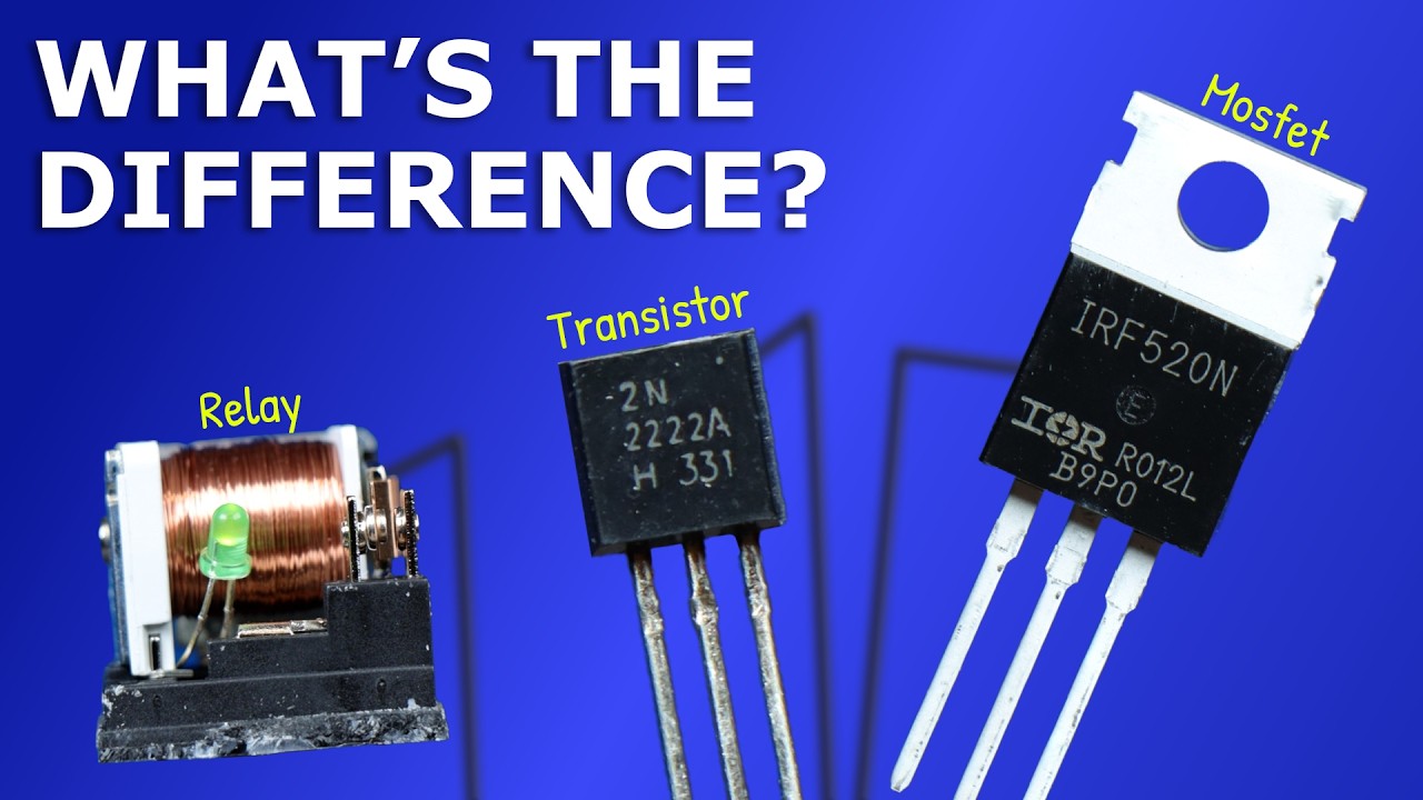
MOSFET vs Transistor vs Relay: Most People Get This Wrong
video description
Date: 2026-07-10
Related videos





Comments and reviews: 20
gillpratt
Also - the reason for series gate resistors on MOSFETS isn't so much to protect the digital circuits driving them from overcurrent, as those circuits usually have limited output pull-up current and output short-circuit protection anyway, and the total charge they must deliver to the gate for a turn-on is the same no matter what the gate series resistor is. Rather, the purpose of the gate series resistor it is to slow down the turn-on of the MOSFET and the dV/dt of the drain current and add a little inherent damping so as to prevent oscillations from parasitic inductances and capacitances. Also, if the output stage of the digital device driving the MOSFET pulls down reliably, you don't need the pull-down resistor you talk about as being essential to turn off the MOSFET. That resistor is there because sometimes during power-up of the whole system, the driving circuit leaves its output floating, so the passive pull-down resistor defaults the MOSFET to off.
reply
Also - the reason for series gate resistors on MOSFETS isn't so much to protect the digital circuits driving them from overcurrent, as those circuits usually have limited output pull-up current and output short-circuit protection anyway, and the total charge they must deliver to the gate for a turn-on is the same no matter what the gate series resistor is. Rather, the purpose of the gate series resistor it is to slow down the turn-on of the MOSFET and the dV/dt of the drain current and add a little inherent damping so as to prevent oscillations from parasitic inductances and capacitances. Also, if the output stage of the digital device driving the MOSFET pulls down reliably, you don't need the pull-down resistor you talk about as being essential to turn off the MOSFET. That resistor is there because sometimes during power-up of the whole system, the driving circuit leaves its output floating, so the passive pull-down resistor defaults the MOSFET to off.
reply
thomasmaughan4798
12: 55 Another aspect of MOSFET is the very low on resistance which is why they can switch higher currents provided you stay out of the linear region. Fully OFF, they experience voltage (source to drain) but no current hence no power dissipation in the device. Fully on you have almost no voltage source to drain, lots of current, and still no power dissipation.
Because the gate is a capacitor you are going to have a small burst of current (electron flow) at the moment of turning on or off. A high frequency switcher will start to consume a noticeable amount of power charging and discharging the gate capacitance.
This is also why the clock frequency of a processor chip (billions of microscopic MOSFETs) has almost everything to do with power consumption. You slow down the clock frequency to conserve power.
reply
12: 55 Another aspect of MOSFET is the very low on resistance which is why they can switch higher currents provided you stay out of the linear region. Fully OFF, they experience voltage (source to drain) but no current hence no power dissipation in the device. Fully on you have almost no voltage source to drain, lots of current, and still no power dissipation.
Because the gate is a capacitor you are going to have a small burst of current (electron flow) at the moment of turning on or off. A high frequency switcher will start to consume a noticeable amount of power charging and discharging the gate capacitance.
This is also why the clock frequency of a processor chip (billions of microscopic MOSFETs) has almost everything to do with power consumption. You slow down the clock frequency to conserve power.
reply
lunalangton5776
1: 29 wait, what did you do to make your relay go bang This was just done for effect right
6: 47 BC327 is a PNP, the mystery SOT223 and other packages only might be a transistor, the labels cannot be read. This is not a competition entry.
7: 35 Although this does work, to provide some nuance, using MOSFETs in linear mode is kind of a waste of a MOSFET and requires staying within a limited safe operating area to avoid Spirito effect with typical parts, you may as well use a BJT for this with the only advantage of the MOSFET being that you CAN fully open it and only pay the Rds(on) instead of the Vbe drop. The region over which you actually have control is very small btw. In reality you should hard-switch a MOSFET with e. g. PWM as shown on the next frame.
reply
1: 29 wait, what did you do to make your relay go bang This was just done for effect right
6: 47 BC327 is a PNP, the mystery SOT223 and other packages only might be a transistor, the labels cannot be read. This is not a competition entry.
7: 35 Although this does work, to provide some nuance, using MOSFETs in linear mode is kind of a waste of a MOSFET and requires staying within a limited safe operating area to avoid Spirito effect with typical parts, you may as well use a BJT for this with the only advantage of the MOSFET being that you CAN fully open it and only pay the Rds(on) instead of the Vbe drop. The region over which you actually have control is very small btw. In reality you should hard-switch a MOSFET with e. g. PWM as shown on the next frame.
reply
lowelldolney2986
Power Systems Electrical Engineer here. Watched to remember the difference between a BJT and MOSFET, but stayed to watch the magic smoke come out!
FYI, in the USA at least we still call protective devices relays because before computers you would have an electromechanical spinning disk that would operate a relay that would operate a VERY large circuit breaker. Nowadays relays are little computers with inputs and outputs (that are also relays, which isn't confusing at all. However, faster modern relays have options to use fast outputs which I think are MOSFETs because they require a pulldown resistor. Typically used on 125VDC control circuits.
Anyway, thanks for the refresher!
reply
Power Systems Electrical Engineer here. Watched to remember the difference between a BJT and MOSFET, but stayed to watch the magic smoke come out!
FYI, in the USA at least we still call protective devices relays because before computers you would have an electromechanical spinning disk that would operate a relay that would operate a VERY large circuit breaker. Nowadays relays are little computers with inputs and outputs (that are also relays, which isn't confusing at all. However, faster modern relays have options to use fast outputs which I think are MOSFETs because they require a pulldown resistor. Typically used on 125VDC control circuits.
Anyway, thanks for the refresher!
reply
gillpratt
Paul - Beautiful hydraulic analogies. However, the explanation of the operation of the collector to base barrier in a BJT is backwards - unless the BJT is saturated, the B to C juction is reverse biased, and thus does not collapse as you said the way the B to E junction does when it is forward biased. Rather the electric field barrier in the reverse biased B to C junction sweeps up the charges injected into the base by the forward biased emitter. This is where the name emitter, base, colelctor come from, which are more functionally descriptive than the older physically descriptive names of cathode, grid, and plate that vacuum tubes used before.
reply
Paul - Beautiful hydraulic analogies. However, the explanation of the operation of the collector to base barrier in a BJT is backwards - unless the BJT is saturated, the B to C juction is reverse biased, and thus does not collapse as you said the way the B to E junction does when it is forward biased. Rather the electric field barrier in the reverse biased B to C junction sweeps up the charges injected into the base by the forward biased emitter. This is where the name emitter, base, colelctor come from, which are more functionally descriptive than the older physically descriptive names of cathode, grid, and plate that vacuum tubes used before.
reply
milasudril
You forgot the triode. This device has similar characteristics as a MOSFET. Triodes are still found high power radio equipment. Some claim that tube amplifiers sounds better. Speaking of amplifiers, BJT: s are usually found in end stage, since they can produce the current needed to drive the speakers. MOSFET: s work well at the input stage, where you want high input impedance.
For logic gates, MOSFET: s are preferable, since the do not load the previous stage. The CMOS design works well because it ideally only draws power when it switches. When the device shrinks, the capacitor starts to leak which must be worked around at nm-scale.
reply
You forgot the triode. This device has similar characteristics as a MOSFET. Triodes are still found high power radio equipment. Some claim that tube amplifiers sounds better. Speaking of amplifiers, BJT: s are usually found in end stage, since they can produce the current needed to drive the speakers. MOSFET: s work well at the input stage, where you want high input impedance.
For logic gates, MOSFET: s are preferable, since the do not load the previous stage. The CMOS design works well because it ideally only draws power when it switches. When the device shrinks, the capacitor starts to leak which must be worked around at nm-scale.
reply
specialK319319
I love your videos and think you have some of the best diagrams/graphics out there. As others have stated, the title of this video is very misleading and I really think you should have added a sentence or two explicitly explaining that a mosfet is a type transistor. It's not as clear as it should be watching this video since it's more of a brief throw away line during it.
For anyone new to this topic, I think it will cause unecessary confusion in an already confusing area. At the very least I would suggest updating the title.
You make great videos though so keep up the good work otherwise.
reply
I love your videos and think you have some of the best diagrams/graphics out there. As others have stated, the title of this video is very misleading and I really think you should have added a sentence or two explicitly explaining that a mosfet is a type transistor. It's not as clear as it should be watching this video since it's more of a brief throw away line during it.
For anyone new to this topic, I think it will cause unecessary confusion in an already confusing area. At the very least I would suggest updating the title.
You make great videos though so keep up the good work otherwise.
reply
mstcrow5429
If it's find the transistor, singular, E4 is definitely a transistor, because part name lookup. The tiny ones are shown as being MOSFETS in video, and the one on the right with three pins but what looks like a heatsink in back is probably a MOSFET. The video considers a MOSFET to not be a transistor, which I assume means it's not a BJT transistor; this is because the Internet tells me that a BJT is better than a MOSFET for applying linear analog signals, and this exact application was shown in the video while discussing transistors.
reply
If it's find the transistor, singular, E4 is definitely a transistor, because part name lookup. The tiny ones are shown as being MOSFETS in video, and the one on the right with three pins but what looks like a heatsink in back is probably a MOSFET. The video considers a MOSFET to not be a transistor, which I assume means it's not a BJT transistor; this is because the Internet tells me that a BJT is better than a MOSFET for applying linear analog signals, and this exact application was shown in the video while discussing transistors.
reply
JustBadMeAndI
That animated relay at 1: 05 does not switch anything, look closely, red wire connected to normally open and the black to normally closed, there’s nothing switched here!
The spring loaded contact should have the red wire connected to it, kinda dumb
Later on it shows an odd animation where the current flows through the block. hahaha, so, the autor knew it wasn’t working but made it seem to work by changing the path of the current through an isolator block.
or insulator
reply
That animated relay at 1: 05 does not switch anything, look closely, red wire connected to normally open and the black to normally closed, there’s nothing switched here!
The spring loaded contact should have the red wire connected to it, kinda dumb
Later on it shows an odd animation where the current flows through the block. hahaha, so, the autor knew it wasn’t working but made it seem to work by changing the path of the current through an isolator block.
or insulator
reply
randy5655
The difference between a FET and a transistor is the internal structure and layering of the P and N type materials. Both are used for switching and amplification. FETs are more efficient and can handle greater power loads than a transistor.
A transistor is either a PNP or an NPN and are either positive or negative applied voltage to turn on or off. The same with FETs.
FET stands for Field Effect Transistor. MOSFET stands for Metal Oxide Silicon FET.
reply
The difference between a FET and a transistor is the internal structure and layering of the P and N type materials. Both are used for switching and amplification. FETs are more efficient and can handle greater power loads than a transistor.
A transistor is either a PNP or an NPN and are either positive or negative applied voltage to turn on or off. The same with FETs.
FET stands for Field Effect Transistor. MOSFET stands for Metal Oxide Silicon FET.
reply
bobvines00
At about 06: 30 or so, you spread a group of transistors out on a gray carpet among other electronic components. I had to turn my screen's brightness up to its maximum (it's a laptop) in order to see things more clearly with old eyes, but here's what I think I saw:
Seven (7) transistors located at: D7, E4, G9, I5, N3, R9, and what appears to be a large transistor with an extra metal (heat sink) pad across squares S2-T2.
reply
At about 06: 30 or so, you spread a group of transistors out on a gray carpet among other electronic components. I had to turn my screen's brightness up to its maximum (it's a laptop) in order to see things more clearly with old eyes, but here's what I think I saw:
Seven (7) transistors located at: D7, E4, G9, I5, N3, R9, and what appears to be a large transistor with an extra metal (heat sink) pad across squares S2-T2.
reply
mizar010
I believe the transistors are are E4 and Q9
E7 is a screw
J7 looks to be a small capacitor
J10 is a resistor
N11 appears to be a diode (I don't see any markings that would make it s resistor in the image)
)3 looks to be a another diode
S2 COULD be a transistor, but I think its actually a MOSFET
T6 appears to be a IC of some type. image is too blurry to see the markings to tell when zoomed in
reply
I believe the transistors are are E4 and Q9
E7 is a screw
J7 looks to be a small capacitor
J10 is a resistor
N11 appears to be a diode (I don't see any markings that would make it s resistor in the image)
)3 looks to be a another diode
S2 COULD be a transistor, but I think its actually a MOSFET
T6 appears to be a IC of some type. image is too blurry to see the markings to tell when zoomed in
reply
BrianTimm
Excellent video as per usual. Even having working alongside electronics for a long time a new perspective helps me understand it better.
Small thing I noticed. 6: 10 you have the collector labeled as P type when it should be N type (it is otherwise animated correctly)
and thanks for showing it in electron flow, conventional current gets confusing once you're talking about semiconductors.
reply
Excellent video as per usual. Even having working alongside electronics for a long time a new perspective helps me understand it better.
Small thing I noticed. 6: 10 you have the collector labeled as P type when it should be N type (it is otherwise animated correctly)
and thanks for showing it in electron flow, conventional current gets confusing once you're talking about semiconductors.
reply
toolman550
The main difference between a bipolar transistor and a mosfet is the bipolar transistor is a current amplifying device where the mosfet is a transconductance device if you remodel each device in H parameters (Hre, Hoe, Hfe) is immediate obvious what the difference between the two devices are in a bipolar device Bata is the current gain and in a Moffett gain is expresed in volts per amp
reply
The main difference between a bipolar transistor and a mosfet is the bipolar transistor is a current amplifying device where the mosfet is a transconductance device if you remodel each device in H parameters (Hre, Hoe, Hfe) is immediate obvious what the difference between the two devices are in a bipolar device Bata is the current gain and in a Moffett gain is expresed in volts per amp
reply
netsendjoe
Brilliant explanations, easy to understand. Interestingly, hardware electronics have a lot in common with software. Could you explain how this works in a programming language I know about switch and case statements, but the transistor sounds more than just an if-and-else or if-or-else. And how exactly do transistors process and amplify sound Those would be interesting to learn.
reply
Brilliant explanations, easy to understand. Interestingly, hardware electronics have a lot in common with software. Could you explain how this works in a programming language I know about switch and case statements, but the transistor sounds more than just an if-and-else or if-or-else. And how exactly do transistors process and amplify sound Those would be interesting to learn.
reply
DarkRavenhaft
I need to get a unit tester.
D7, E4 (assuming it isn't a sensor package, G9, I5, N3, R9, ST2, and possibly T6 but it's difficult to be certain without the IC package P/N.
Now try playing this game with 1/72 plastic models over high-pile carpet in hide-the-stains apartment special. No magnet will save you.
reply
I need to get a unit tester.
D7, E4 (assuming it isn't a sensor package, G9, I5, N3, R9, ST2, and possibly T6 but it's difficult to be certain without the IC package P/N.
Now try playing this game with 1/72 plastic models over high-pile carpet in hide-the-stains apartment special. No magnet will save you.
reply
Mattmik1853
Wait, N-type having phosphorus and P-type having boron reversing it would be much easier to remember just alphabetically, but physics said no. 5: 53 Phosphorus has 5 valence electrons (donates an electron = N-type) and Boron has 3 (leaves a hole = P-type. Nature really missed a great mnemonic opportunity there!
reply
Wait, N-type having phosphorus and P-type having boron reversing it would be much easier to remember just alphabetically, but physics said no. 5: 53 Phosphorus has 5 valence electrons (donates an electron = N-type) and Boron has 3 (leaves a hole = P-type. Nature really missed a great mnemonic opportunity there!
reply
alanhilder1883
The relay can isolate a control circuit power supply from the Load circuit power supply. ( can be different voltages, AC/DC air guitar differences ) The Electronic versions need there to be a connection between both and are DC only ( may be set up in a pos/neg setup I think.
reply
The relay can isolate a control circuit power supply from the Load circuit power supply. ( can be different voltages, AC/DC air guitar differences ) The Electronic versions need there to be a connection between both and are DC only ( may be set up in a pos/neg setup I think.
reply
danieljurgill1681
Do the diagrams in this video show the current flow direction in conventional terms or in electron motion Both the Collector and Emitter, and the Source and Drain make it confusing enough.
So do electrons flow from collector to emitter, and from source to drain
reply
Do the diagrams in this video show the current flow direction in conventional terms or in electron motion Both the Collector and Emitter, and the Source and Drain make it confusing enough.
So do electrons flow from collector to emitter, and from source to drain
reply
Gameplayer55055
Also, NPN regions aren't the same size in a BJT transistor. Usually collector is bigger than emitter and swapping them would give you horrible hFE
JFET source and drain can be swapped (with some exceptions. MOSFET can't be swapped because of a parasitic diode.
reply
Also, NPN regions aren't the same size in a BJT transistor. Usually collector is bigger than emitter and swapping them would give you horrible hFE
JFET source and drain can be swapped (with some exceptions. MOSFET can't be swapped because of a parasitic diode.
reply
Add a review, comment
Other channel videos